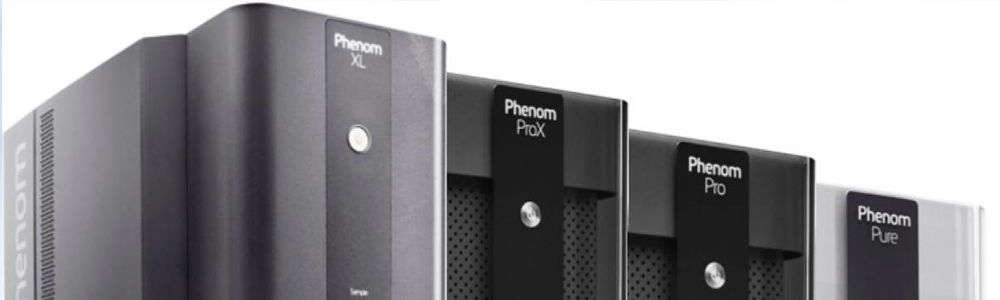
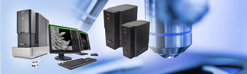
logo

Hotline: +8424 62967539  |  ADD: RM 630, 6th Floor, CIC Tower, No. 2 Nguyen Thi Due Str., Cau Giay, Ha Noi, Vietnam.

sl33
sl44
upt_animation_column_failure
cimps-qe-ipce_wb

Phenom ProX G6

Phenom ProX G6
phenom-prox-g6 - ảnh nhỏ  1

Phenom ProX G6

The sixth-generation of Thermo Scientific Phenom ProX G6 Desktop SEM fills the gap between light microscopy and floor-model SEM analysis, thus expanding the capabilities of research facilities. It offers fast, high-resolution imaging in addition to an integrated energy-dispersive X-ray diffraction (EDS) detector for robust, easy-to-use, rapid elemental analysis.

prox

Key Features

Fast and easy to use

The Phenom Pro Desktop SEM can be used to relieve the burden of routine analysis for common samples from floor-model SEM instruments. Instrument configuration and the sample loading mechanism ensure quick imaging with minimal time spent tuning between experiments.

Long-lifetime CeB6 source

Facility users of any experience level can quickly begin producing high-quality results with the Phenom Pro Desktop SEM. Its long-lifetime CeB6 source offers high brightness while requiring low maintenance.

Robust and small form factor

It's high stability and small form factor allow the instrument to be used in practically any lab environment; more simply put, it does not require specialized infrastructure or expert oversight.


Specifications

Light optical magnification
  • 20–134x
Electron optical magnification range
  • 160-350,000x
Resolution
  • ≤ 6 nm SED and ≤ 8 nm BSD
Digital zoom
  • Max. 12x
Light optical navigation camera
  • Color
Acceleration voltages
  • Default: 5 kV, 10 kV and 15 kV
  • Advanced mode: adjustable range between 4.8 kV and 20.5 kV imaging and analysis mode
Vacuum modes
  • High vacuum mode
  • Charge reduction mode via optional low vacuum sample holder
Detector
  • Backscattered electron detector (standard)
  • Energy-dispersive X-ray detector (standard)
  • Secondary electron detector (optional)
Sample size
  • Up to 25 mm diameter (optional 32 mm)
Sample height
  • Up to 35 mm (optional 100 mm)
Desktop SEM blog

Desktop SEM Blogs

Want to unlock the great power of scanning electron microscopy without having to compromise on usability? Enhance your knowledge on Scanning Electron Microscopy and find out how Desktop SEM can optimally support your research in our Phenom Desktop SEM blogs.

Learn more

Applications

Process Control_Thumb_274x180_144DPI

Process Control
 

Modern industry demands high throughput with superior quality, a balance that is maintained through robust process control. SEM and TEM tools with dedicated automation software provide rapid, multi-scale information for process monitoring and improvement.


Quality Control_Thumb_274x180_144DPI

Quality Control
 

Quality control and assurance are essential in modern industry. We offer a range of EM and spectroscopy tools for multi-scale and multi-modal analysis of defects, allowing you to make reliable and informed decisions for process control and improvement.


Fundamental Materials Research_R&D_Thumb_274x180_144DPI

Fundamental Materials Research

Novel materials are investigated at increasingly smaller scales for maximum control of their physical and chemical properties. Electron microscopy provides researchers with key insight into a wide variety of material characteristics at the micro- to nano-scale.


pathfinding_thumb_274x180_144dpi

Semiconductor Pathfinding and Development

Advanced electron microscopy, focused ion beam, and associated analytical techniques for identifying viable solutions and design methods for the fabrication of high-performance semiconductor devices.

yield_ramp_metrology_2_thumb_274x180

Yield Ramp and Metrology

We offer advanced analytical capabilities for defect analysis, metrology, and process control, designed to help increase productivity and improve yield across a range of semiconductor applications and devices.

Semiconductor Failure Analysis

Semiconductor Failure Analysis

Increasingly complex semiconductor device structures result in more places for failure-inducing defects to hide. Our next-generation workflows help you localize and characterize subtle electrical issues that affect yield, performance, and reliability.

physical_characterization_thumb_274x180_144dpi

Physical and Chemical Characterization

Ongoing consumer demand drives the creation of smaller, faster, and cheaper electronic devices. Their production relies on high-productivity instruments and workflows that image, analyze, and characterize a broad range of semiconductor and display devices.

SEARCH
SUPPORT ONLINE
icon  +8424 62967539
PARTNER LOGO
8
3
9
zahner_logo_4c_crimson
logo

GSEM., JSC

Tel: +8424 62967539; Email: sales@gsemvn.com

Head Office: RM 630, 6th Floor, CIC Tower, 1 Nguyen Thi Due Str., Cau Giay Dist., Hanoi, Vietnam.

Registered Address: No. 18 Alley 313/6 Lane 313 Linh Nam, Hoang Mai, Hanoi